Effective PCB (Printed Circuit Board) design is a key part of the production of any electronic device. With aspects such as understanding the specifics of the PCB, design with assembly in mind, optimized signal paths, testing and quality control, as well as continuous cooperation with the customer, it is possible to achieve not only high performance, but also product reliability.
PCBs – manufacturing material
.
The basis of any electronic device is the PCB, which connects various components together to form a complex circuit. Choosing the right material, thickness and number of layers is crucial to the functionality and performance of the PCB. Commonly used materials include:
- composite laminates,
- glass-epoxy laminates,
- glass-teflon laminates,
.
.
.
This is due to their good insulating properties and resistance to high temperatures. It is also important to keep in mind the proper selection of PCB material in terms of thermal conductivity and mechanical resistance, which has a direct impact on the durability and reliability of the electronic device. Designers at EMS ELEKTRONIX take these factors into account, ensuring that each PCB is perfectly tailored to the project specifications and customer expectations.
Design with assembly in mind
.
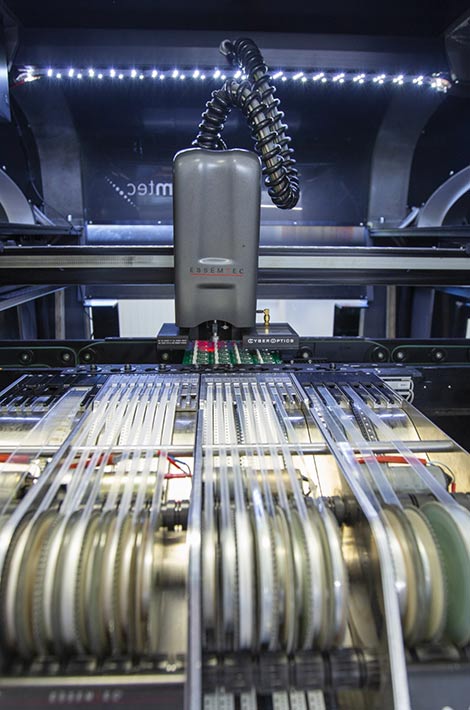
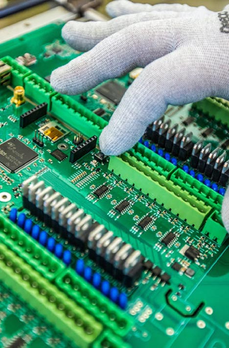
When designing a PCB, it is important to take into account the assembly process of components, whether SMD or THT. Care should be taken to ensure proper component placement to provide easy access for assembly tools and minimize the risk of errors. This strategy also includes planning optimal paths for wires and connectors, making the later stages of PCB assembly much easier. This approach minimizes the need for later adjustments and ensures faster project completion. At EMS ELEKTRONIX, we use state-of-the-art assembly lines and soldering robots that guarantee high precision and efficiency, while reducing the risk of human error.
Optimized PCB signal paths
.
Efficient placement of signal paths is key to ensuring the stability and performance of PCBs. Long paths should be avoided and adequate separation between signals should be ensured to minimize interference and coupling. Special techniques are used in PCB manufacturing, such as introducing reference layers or using more layers to manage signals efficiently. Adjusting the thickness of the paths and their placement to minimize resistance and increase conductivity can significantly improve board performance. At EMS ELEKTRONIX, designers use advanced electrical simulation software, allowing signal paths to be precisely designed even before production begins.
The importance of simulation and modeling in PCB design
.
In modern PCB design, electrical and thermal simulation software plays a key role, enabling designers to accurately model and analyze their designs even before physical prototyping. With advanced simulation tools, it is possible to detect potential problems early on, such as component overheating, insufficient conductivity of paths or the risk of electromagnetic interference. Simulations make it possible to optimize the signal path and assess the impact of different material configurations, which has a direct impact on the efficiency and reliability of the final product. In practice, this means a significant reduction in the time required for design iterations and a reduction in the costs associated with prototype production.
Data management and design documentation
.
Accurate documentation of PCB designs and effective management of data and documentation changes are indispensable elements of the design process, with a direct impact on the quality, efficiency and repeatability of production. Good practices in this area, including the use of IPC standards for PCB documentation and specifications, ensure that all information is clearly defined, easy to understand and accessible to all members of the design and production team. At EMS ELEKTRONIX, special emphasis is placed on keeping the design database up to date, which allows necessary information to be found quickly and makes it easier to make changes or updates to projects.
Testing and quality control
.
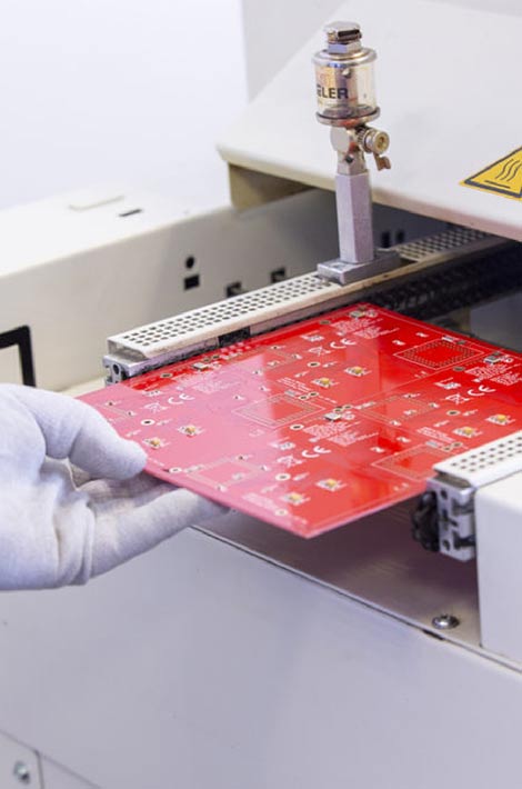
Each printed circuit board goes through a series of tests and quality checks before being delivered to the customer to ensure that all connections work properly and the product is free of defects. At EMS ELEKTRONIX, we use advanced AOI (Automated Optical Inspection) equipment to analyze and point out possible errors at each stage of PCB production, allowing us to intervene quickly and ensure the highest quality of finished boards. In addition, we use functional tests that simulate the actual operating conditions of the device, making it possible to detect and solve problems that might not be noticed during standard inspection tests.
Continuous cooperation with the customer
.
PCB design and manufacturing are processes that require continuous cooperation between the customer and the manufacturer. We are always in direct contact with our customers, offering individual advice and technical assistance at every stage of the project. Thanks to our experience and commitment, customers can count on products fully tailored to their needs and requirements. This approach makes it possible not only to tailor the PCB to the specific needs of the application, but also provides the flexibility to respond to any changes in the design.
PCB design requires not only deep technical knowledge and experience, but also the use of modern tools and techniques, such as electrical and thermal simulation software and precise management of data and design documentation. By applying best practices and constantly striving for excellence, companies like EMS ELEKTRONIX can not only meet but exceed their customers’ expectations, delivering products that are not only functional but also reliable.